Electronics &semiconductor
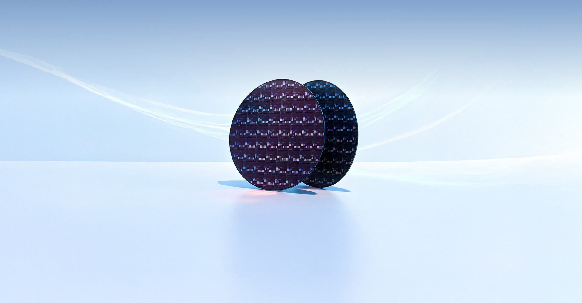
Enabling the precision of digital future with innovative materials

Enabling the precision of digital future with innovative materials
Why ZYPEEK for Electronics &semiconductor?
In semiconductor and electronics manufacturing, ZYPEEK is valued for its high purity, low outgassing, temperature resistance, and dimensional stability. It supports critical applications such as wafer handling, test sockets, and insulation components. With chemical resistance and optional electrostatic dissipative properties, ZYPEEK helps minimize electrostatic damage, enabling higher yields and reliable performance.


Exhibiting high tensile and flexural strength with exceptional creep resistance, ZYPEEK combines rigidity with toughness. It delivers outstanding fatigue resistance under alternating stress and superior wear resistance for an extended service life. Reinforced ZYPEEK grades offer even higher mechanical performance.

Withstands -40°C to 260°C for continuous operation and maintains superior dimensional stability at short-term peaks of 300°C. Inherently self-extinguishing (UL 94 V-0) and halogen-free, this material ensures minimal smoke and zero toxic or corrosive emissions for maximum safety.

Delivers stable electrical insulation with excellent high-voltage and dielectric breakdown resistance. Featuring high dielectric strength and low dielectric loss at high frequencies, it is ideal for demanding insulation components in the semiconductor industry.

ZYPEEK maintains exceptional wear resistance with minimal mass loss under high-temperature friction. Metallic ion contamination remains well below threshold limits, and the material remains free of halogen or other outgassing at high temperatures, effectively safeguarding wafer yield.

Highly resistant to most acids, bases, and organic solvents (except concentrated sulfuric acid). It maintains stable performance in harsh semiconductor environments—even under high heat and humidity—with low water absorption and superior hydrolysis resistance.

Versatile processing via injection molding, extrusion, coating, 3D printing, or CNC enables the production of semi-finished or high-precision parts for any design. One-step injection molding with superior mold release further streamlines production by reducing secondary operations and process steps.
The Future of Electronics & Semiconductor
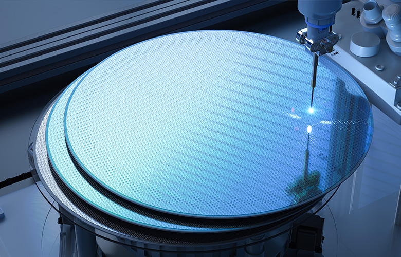
As chip nodes shrink and 3D packaging evolves, harsh process environments are pushing material limits. To meet the soaring demand for HPC, AI, and IoT, manufacturers must balance heat resistance, purity, dimensional stability, and lightweighting. Our answer lies in advanced materials that play a critical role in wafer grinding, handling, and storage solutions.
Our material solutions—featuring high-temperature stability, ultra-low metallic leaching, and superior dimensional stability—are mass-production proven in critical components such as wafer carriers, IC test sockets, CMP retaining rings, and selective plating rings. By partnering with equipment and device manufacturers, we accelerate the transition from process validation to full-scale production, delivering solutions with higher process yields and lower contamination risks for next-generation packaging.
ZYPEEK Applications in Semiconductor Systems
Leveraging advanced PEEK technology, we provide comprehensive solutions for semiconductor equipment, wafer fabrication, and packaging & testing—covering design, material validation, performance optimization, and specialized technical support.
We look forward to partnering with engineering teams at OEMs and wafer fabs to co-develop and industrialize next-generation chip processes and advanced packaging applications.


ZYPEEK Grades Recommended for Electronics & Semiconductors